


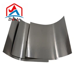
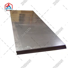



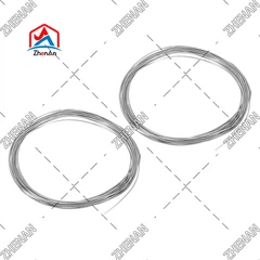


Common specifications of pure nickel strip include wide band 2-330mm, thickness 0.05-1mm, and length greater than or equal to 3000mm.
Thin layer nickel strip thickness is usually less than 0.1mm, and is often used in the manufacture of microelectronic components; thick layer nickel strip thickness is more than 0.1mm, and is mostly used for battery separators, etc.
Nickel Strip Product Basic Parameters
|
Grade |
Ni+Co |
As |
Bi |
C |
Cd |
Cu |
Fe |
Mg |
Mn |
|
Ni201
Ni200 |
≥99,9
≥99,5 |
≤0,001
≤0,002 |
≤0,001
≤0,02 |
≤0,01
≤0,1 |
≤0,001
≤0,002 |
≤0,015
≤0,1 |
≤0,04
≤0,1 |
≤0,01
≤0,1 |
≤0,002
≤0,05 |
|
|
P |
Pb |
S |
Sb |
Si |
Sn |
Zn |
Impurity |
|
|
Ni201
Ni200 |
≤0,001
≤0,002 |
≤0,001
≤0,002 |
≤0,001
≤0,005 |
≤0,001
≤0,002 |
≤0,03
≤0,15 |
≤0,001
≤0,002 |
≤0,005
≤0,007 |
≤0,1
≤0,5 |
|
Nickel Strip Product Display


We are your best and most assured choice:
1. Professional and timely pre-sales consulting team
2. One-to-one sales support team
3. Professional manufacturing team
4. Butler-style after-sales service team
FAQ About ZhenAn
Q: How long is your delivery time?
A: Samples only take 1 day, and mass production time for order quantity over 100 kg takes 2-3 days.
Q: How do you ship and how long does it take to arrive?
A: Sample orders are usually shipped by DHL, UPS, FedEx or TNT. It usually takes 4-5 days to arrive. Air and sea shipping are also available for formal orders.
Q: Can my logo be printed on the solder bar/package?
A: Yes. Please inform us formally before production and confirm the design based on our samples first.